
trends in printed circuit prototype manufacturing
PCBs are a vital part of many electronic devices, from laptops and smartphones to medical equipment and industrial machines. They connect components and provide the necessary electrical power to operate a device. Printed circuit boards are often made of multiple layers of insulating and conductive materials glued together. Some are double-sided, while others have as many as 30 layers of conductive copper. Each layer contains a pattern of conductors that form the circuit and link to each other through plated holes called vias.
Technological innovations and emerging trends are shaping the future of printed circuit prototype manufacturing and assembly. These include miniaturization, high-density interconnect PCBs, sustainable materials, and IoT integration. Staying informed and adapting to these trends is crucial for businesses in the electronics industry.
Miniaturization: Modern consumers are increasingly demanding smaller and more lightweight electronic products, including PCBs. As a result, manufacturers are focusing on making PCBs as small as possible while maintaining their functionality and performance. This is facilitated by new technology and advanced materials, such as high-frequency laminates and flexible substrates. It is also driven by the growing use of PCBs in portable devices like laptops and smartphones.
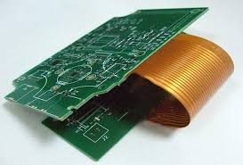
What are the trends in printed circuit prototype manufacturing?
Increasing demand for compact and lightweight electronic devices has also led to the growth of high-density interconnect PCBs (HDI). HDI PCBs feature denser circuitry than traditional PCBs, with 120-160 pins per square inch. These PCBs are able to achieve this density by using blind, buried, and micro-vias — plated holes that connect different layers without passing through the surface of the board. They also use smaller components and less space to house them, further reducing the overall size of the product.
Sustainable practices and eco-friendly procedures are another big trend in PCB production. These practices help reduce the environmental impact of electronic manufacturing while also lowering production costs and improving quality. Some of the most important trends in this area include using recycled materials, using reusable chiplet functions, and eliminating waste from the manufacturing process.
Automation and robotics are other big trends in the PCB manufacturing and assembly industry. These technologies streamline the production process and improve efficiency by reducing human error, allowing for faster turnaround times, and guaranteeing consistent quality.
Testing and inspection technologies are also gaining traction in the industry. These technologies include X-ray and automated optical inspection, which can identify defects and faults in the board early on. This helps reduce the number of defective products, and it also makes it easier for people to work with complicated layouts and diverse components.
Another emerging trend is the increased use of commercial off-the-shelf (COTS) components in critical systems, such as in aerospace and military applications. COTS parts are cheaper than custom-designed components and can save significant time and money during the manufacturing and assembly process. However, the proliferation of these parts could potentially compromise the reliability of the finished product. Manufacturers are working to mitigate this risk by using advanced software and simulation tools to analyze and predict potential problems before they occur.

+ There are no comments
Add yours