
PCB Printed Circuit Boards
From mission-critical defense electronics to consumer gadgets, pcb printed circuit boards make it possible to connect and operate the devices we use every day. They provide the wireless connectivity and high-frequency circuitry that enable the latest applications and products, including advanced technologies like Bluetooth, Wi-Fi, and cellular connectivity. These PCBs are often constructed from a variety of materials and are either rigid or flexible. The choice of the board material depends on tradeoffs between cost, electrical performance, thermal properties, and manufacturability based on the target application.
RF PCBs require special considerations for conducted emissions and immunity compliance. In general, these requirements are met by routing RF signals to dedicated layers and inserting decoupling capacitors. The board layout must be carefully reviewed to identify potential sources of interference noise or transients that could couple to other conductors on the PCB and/or cables connecting to it. Typically, the first step is to locate all I/O connectors on one edge of the board if possible, as this will minimize coupling from RF signals to other parts of the circuit. The board should also contain enough solid ground plane layers to ensure that return currents from RF signals come back directly above and below the signal trace.
Choosing a pcb printed circuit board material that has a stable dielectric constant value is critical for RF applications. FR-4 (epoxy resin with glass reinforcement) has been the standard for PCBs for many years, but high-frequency applications are pushing the limits of this material. Rogers Advanced Connectivity Solutions offers a range of specialized laminates that are usable in RF and microwave frequencies with excellent stability.
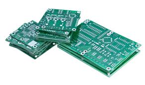
Using PCB Printed Circuit Boards in RF Applications
The design of the PCB itself is also important. This includes the selection of components and footprints, the creation of a CAD file of the circuit board, and the placement of the traces on the board. It is also important to consider the thermal behavior of the PCB, as some RF components generate heat.
Once the schematic is completed, the CAD file can be used to create a physical drawing of the circuit board. This process is called “tracing” and is done with a software program that compares the circuit diagram to the actual circuit board. The program will then determine where the copper pads and through-hole connections will be positioned on the board. The resulting file can then be sent to the manufacturer for production.
RF PCBs are typically multi-layer and have large areas of solid copper planes for conducting power and signal lines. RF signal traces should be routed on separate layers from DC power lines to reduce parasitic inductance and capacitance. The traces should be sized to accommodate the maximum current expected, and they should have via holes sized to reduce signal loss. Care should be taken to avoid forming loops around the pins of I/O connectors, as these can contribute significantly to interference problems.

+ There are no comments
Add yours